


Occasions
Divisions
Performances
Occasions
Divisions
Performances
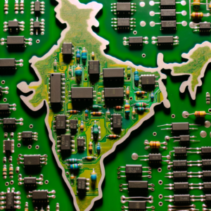
India is set to produce not only semiconductors but also chip-fabrication tools, according to IT Minister Ashwini Vaishnaw. The nation's plan is to produce all necessities for creating semiconductors, including factories, chemicals, and machinery. Vaishnaw believes that the production of chip-fabrication equipment will significantly enhance India's presence in the international semiconductor arena.
India is preparing to develop its own semiconductor manufacturing tools, says IT Minister Ashwini Vaishnaw. During the inauguration of the Applied Materials' India Validation Centre in Bengaluru, Vaishnaw emphasized that India is set to produce all the necessary components for semiconductor production, including fabrication plants, chemicals, and machinery.
According to a report by the Economic Times, Applied Materials has put $20 million into the center, which is expected to provide jobs for 500 individuals.
The IT minister asserted that the whole semiconductor production network, encompassing fabrication plants, ATMP units, chemicals, gases, substrate, consumables, and equipment related to semiconductor production, will be manufactured in India.
Applied Materials also disclosed plans to invest $400 million over a span of four years to set up a semiconductor manufacturing technology engineering hub in Bengaluru.
The minister also highlighted that deals established during the Prime Minister's trip to the US have borne fruit, encompassing the initiation of Micron's ATMP building and LAM Research's Semiverse Solutions for instructing semiconductor engineers.
Additionally, Applied Materials plans to set up a facility in India according to the agreements, and AMD has launched a design center in Bengaluru. These advancements indicate notable growth in India's semiconductor sector.
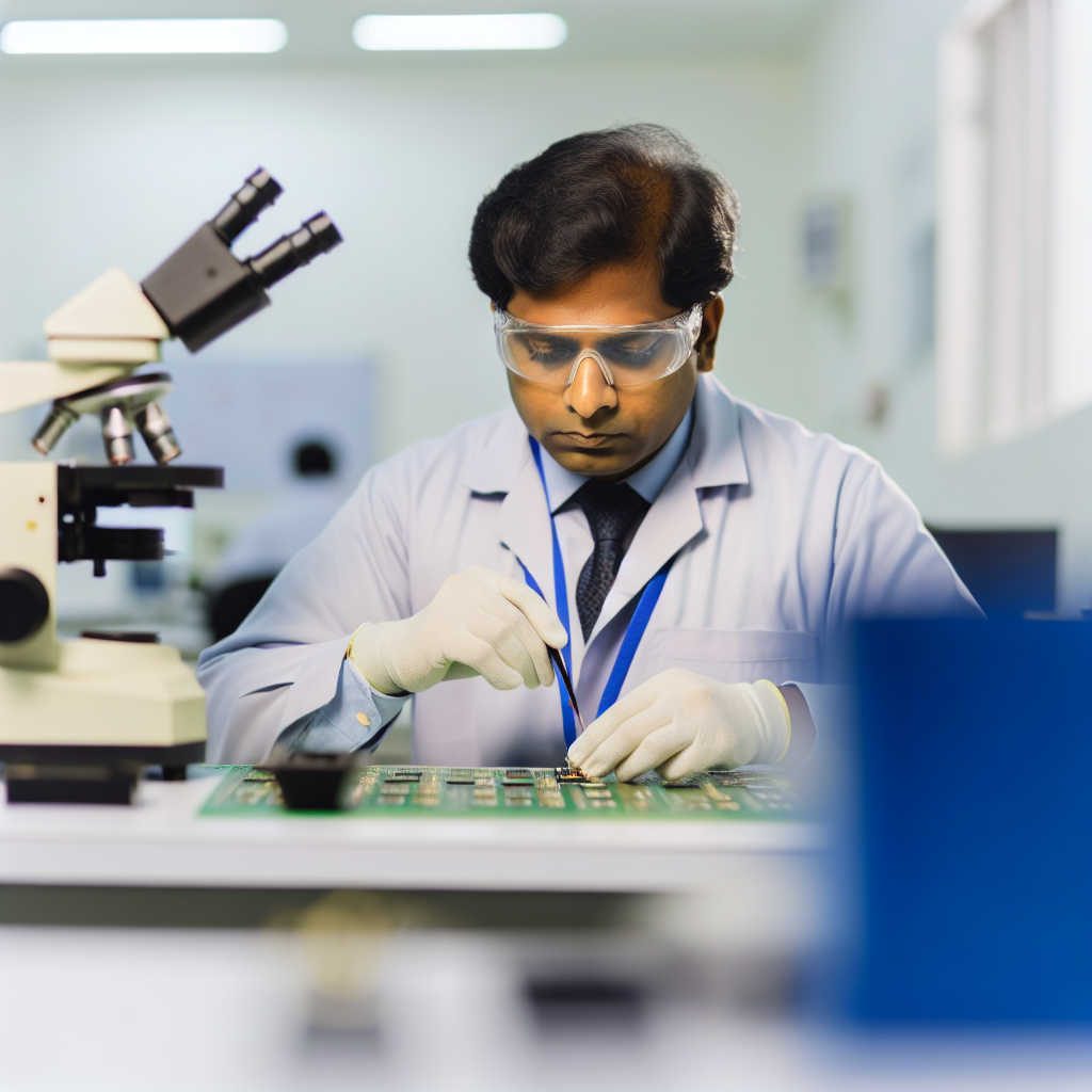
Sonny Kunnakkat, who is the managing director of Worldwide Operations at Applied Materials' Advanced Manufacturing Technology, announced that the recently set up facility in India will be the first privately owned one with the ability to process 300 mm wafers. This represents a considerable improvement from the country's earlier capacity to process 200 mm wafers.
The Indian Institute of Technology (IIT) has confirmed the presence of a 300 mm processing unit. However, Kunnakkat stressed that this latest facility serves business purposes rather than educational ones. Applied Materials will carry out its own research and development in this location, concentrating on machinery for chip production. The wafers created here will not be sold; instead, they'll be used in the company's own machines to support their clients' chip production processes.
Kunnakkat emphasized the swift progression of equipment advancement, which requires constant innovation to meet the changing demands of customers. He insisted that this innovation will be a primary objective at the new center.
Kunnakkat pointed out that the semiconductor hardware system in India is still at a very early stage. He stressed the importance of a well-rounded support system, which includes managing the supply chain, material handling, logistics, and crucial utilities such as water and electricity, to guarantee the survival and durability of semiconductor factories in the nation.
He also stressed the significance of cooperation between ecosystem participants to expand semiconductor production in India, highlighting the need for these operations to be larger to satisfy industry requirements. Applied Materials is collaborating closely with the government to aid in this expansion process.
Kunnakkat elaborated on the plans to establish the company's engineering hub in Bengaluru. He stated that they have a ten-acre plot earmarked for this project. The construction of this complex facility is currently in the design phase. Since they lack the necessary design expertise in India, they're sourcing it from various global locations. However, he clarified that this process won't be completed in the next half-year.
Kunnakkat emphasized the deficiency of process engineering thinking and the inexperience in setting up and starting semiconductor equipment in India. He noted that the firm had to recruit professionals from Singapore and Taiwan, who are experts in these roles, to operate at its India Validation Centre.
(Incorporating information from various sources)
Search for us on YouTube
Top Programs
Associated Articles
Rising Bharat Summit 2024: Indian-made Semicon set to enter the market by December 2024, according to IT Minister Ashwini Vaishnaw
Rising Bharat Summit 2024: India emerges as a significant export hub, Congress squandered four decades, states IT Minister Ashwini Vaishnaw
Indian Government greenlights Tata Group's Rs 91,000 crore chip foundry, slated for construction in Dholera, Gujarat
The next innovation surge in India will be driven by semiconductors and AI, predicts IT Minister Rajeev Chandrasekhar
Rising Bharat Summit 2024: Semiconductors manufactured in India are projected to be available by December 2024, says IT Minister Ashwini Vaishnaw
Rising Bharat Summit 2024: India has become a key export center, with the Congress party wasting forty years, claims IT Minister Ashwini Vaishnaw
The Indian Government has approved Tata Group's plan for a Rs 91,000 crore chip foundry in Dholera, Gujarat
The future of innovation in India is expected to be shaped by semiconductors and AI, according to IT Minister Rajeev Chandrasekhar
Available on YouTube
Firstpost holds all rights, protected by copyright, as of 2024


+ There are no comments
Add yours