


Activities
Divisions
Performances
Activities
Divisions
Performances
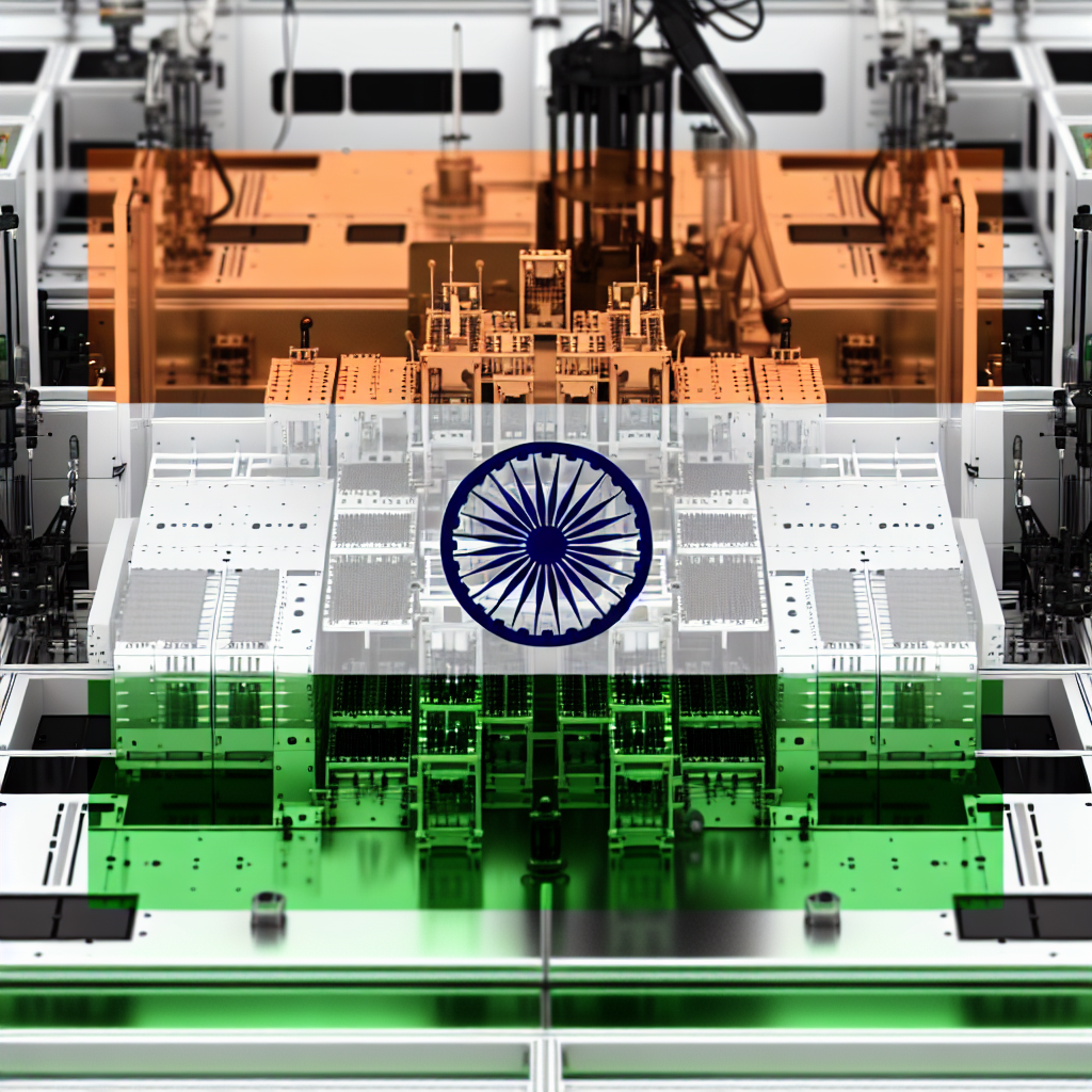
India won't just produce semicon chips, but will also start creating chip-making machinery, according to IT Minister Ashwini Vaishnaw. India's goal is to produce every required component for semiconductor production such as fabs, chemicals, and equipment. IT Minister Ashwini Vaishnaw stated that manufacturing chip-making tools will significantly enhance India's reputation as a key participant in the global semiconductor industry.
India is preparing to create its own semiconductor manufacturing equipment, as revealed by IT Minister Ashwini Vaishnaw. Vaishnaw, during the inauguration of the Applied Materials' India Validation Centre in Bengaluru, emphasized that India will manufacture all the necessary components for semiconductor production, such as fabs, chemicals, and equipment.
Applied Materials has funneled $20 million into the center, which is projected to provide jobs for 500 individuals, according to a publication from the Economic Times.
The IT minister has asserted that all aspects of the semiconductor industry, including fabrication units, assembly, testing, packaging and manufacturing materials such as chemicals, gases, substrate, consumables and equipment, will be produced in India.
Furthermore, Applied Materials declared a commitment to invest $400 million over a span of four years to set up a semiconductor manufacturing technology engineering hub in Bengaluru.
The minister also highlighted that the deals signed during the Prime Minister's visit to the US have been successfully implemented. This includes the beginning of construction of Micron's ATMP and the launch of LAM Research's Semiverse Solutions for training semiconductor engineers.
In addition, Applied Materials plans to set up a facility in India under the agreement, while AMD has launched a design hub in Bengaluru. These advancements symbolize substantial growth in India's semiconductor sector.
Sonny Kunnakkat, the managing director of Advanced Manufacturing Technology, Worldwide Operations at Applied Materials, has declared that the newly formed facility in India will be the first private entity capable of handling 300 mm wafers. This is a substantial step forward from the country's earlier capability of processing 200 mm wafers.
Recognizing the presence of a 300 mm processing unit at the Indian Institute of Technology (IIT), Kunnakkat underscored that this new unit is business-oriented rather than educational. Applied Materials will carry out its own innovation work at this location, concentrating on machinery for semiconductor fabrication. The wafers made will not be sold, but instead, will be utilized within the firm's machinery to support their clients in semiconductor production.
Kunnakkat emphasized the quick pace of equipment innovation, which requires ongoing advancements to meet changing client demands. He insisted that this continual development will be a primary attention point at the new establishment.
Kunnakkat pointed out that the semiconductor hardware environment in India is still quite nascent. He stressed the importance of having a robust support system, which encompasses supply chain management, material handling, logistics, and crucial resources such as water and electricity, to guarantee the durability and lifespan of semiconductor factories in the nation.
He stressed the need for teamwork among ecosystem participants to expand semiconductor production in India, highlighting the crucial need for bigger facilities to fulfill industry requirements. Applied Materials is partnering with the government to streamline this expansion process.
Kunnakkat elaborated on the establishment of the company's engineering hub in Bengaluru, stating, "We've set aside ten acres of land for its construction. The project is complex and still in the design phase. We currently lack the necessary design expertise in India, necessitating the recruitment of specialists from various global locations. However, this won't be achieved in the next six months."
Kunnakkat underscored the lack of a systematic approach towards engineering and the deficiency in experience related to setting up and initiating semiconductor tools in India. He noted that the firm had to recruit professionals from Singapore and Taiwan, who have expertise in these areas, to operate at its India Validation Centre.
(Incorporating information from various sources)
Look for us on YouTube
Popular Broadcasts
Associated Articles
The Rising Bharat Summit 2024 announces that semiconductors made in India will be available in the market by December 2024, according to IT Minister Ashwini Vaishnaw.
At the Rising Bharat Summit 2024, IT Minister Ashwini Vaishnaw declared India as a significant export center, criticizing the Congress for wasting four decades.
The Indian Government has given the green light for Tata Group's Rs 91,000 crore chip foundry, which is planned to be established in Dholera, Gujarat.
The next innovation wave in India is expected to be driven by semiconductors and artificial intelligence, says IT Minister Rajeev Chandrasekhar.
You can also find this on YouTube.
Firstpost holds all rights and is protected by copyright as of 2024


+ There are no comments
Add yours