


Occasions
Divisions
Performances
Occasions
Divisions
Performances
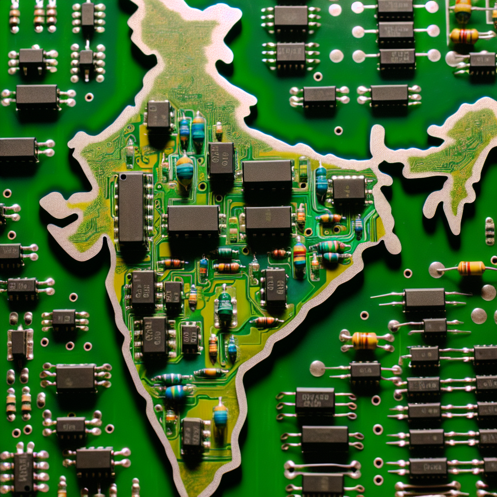
India is planning not only to produce semiconductor chips but also to venture into the creation of chip-making machinery, according to IT Minister Ashwini Vaishnaw. The goal is to locally produce all necessities for semiconductor creation, such as fabs, chemicals, and devices. Vaishnaw stated that the manufacture of chip-making machinery would significantly enhance India's global standing in the semiconductor industry.
IT Minister Ashwini Vaishnaw announced that India is preparing to produce its own equipment for semiconductor manufacturing. Vaishnaw made this statement at the inauguration of the Applied Materials' India Validation Centre in Bengaluru, emphasizing that India is now capable of producing all the necessary components for semiconductor production, such as fabs, chemicals, and equipment.
According to a report by the Economic Times, Applied Materials has invested $20 million in a centre that is set to employ 500 individuals.
The IT minister asserted that the complete semiconductor infrastructure, including fabrication units, ATMP units, chemicals, gases, substrate, consumables, and equipment for making semiconductors, will be produced in India.
Furthermore, Applied Materials has declared that they will invest $400 million over a period of four years to set up a semiconductor manufacturing technology engineering hub in Bengaluru.
The minister also noted that the commitments made during the Prime Minister's visit to the United States have been fulfilled. This includes the start of construction for Micron's ATMP and the initiation of LAM Research's Semiverse Solutions for training semiconductor engineers.
Additionally, Applied Materials plans to set up a hub in India according to the agreements, while AMD has launched a design centre in Bengaluru. These advancements indicate considerable growth in India's semiconductor sector.
Sonny Kunnakkat, who is the managing director of Worldwide Operations at Applied Materials’ Advanced Manufacturing Technology, has announced that the newly opened site in India will be the first privately-run facility able to process 300 mm wafers. This is a notable step forward from the country's former 200 mm wafer processing ability.
Recognizing the presence of a 300 mm processing unit at the Indian Institute of Technology (IIT), Kunnakkat stressed that this new unit is more business-oriented than educational. Applied Materials will carry out its own research and development in this facility, concentrating on machinery for chip production. The wafers produced here won't be marketed, but instead will be utilized internally to support the company's clients with chip manufacturing.
Kunnakkat underscored the swift pace of equipment advancement, which requires ongoing progress to meet the changing demands of customers. He emphasized that such progress will be a major attention point at the new establishment.
Kunnakkat pointed out that India's semiconductor hardware system is still in its early stages. He stressed the importance of a wide-ranging support system, encompassing aspects such as supply chain administration, material management, logistics, and vital resources like water and electricity, to guarantee the durability and lifespan of semiconductor factories in the nation.
He also highlighted the significance of teamwork between ecosystem participants to expand semiconductor production in India, stressing the need for these facilities on a grander scale to satisfy industry requirements. Applied Materials is actively cooperating with the government to ease this expansion process.
Kunnakkat spoke about setting up the company's engineering center in Bengaluru and said, "We possess a ten-acre plot where we plan to establish it. It's a complex structure that we're in the process of designing. Currently, we lack the necessary design experts in India. We're therefore importing skills from various global regions. However, this won't be accomplished within the coming half-year."
Kunnakkat emphasized that India lacked a systematic approach to engineering and experience in setting up and initiating semiconductor tools. He noted that the company had to employ experts from Singapore and Taiwan, who are skilled in these areas, to operate at its India Validation Centre.
(Incorporating information from various sources)
Search for us on YouTube
Highlighted Programs
Associated Articles
During the 2024 Rising Bharat Summit, IT Minister Ashwini Vaishnaw announced that an Indian-made Semicon would be available in the market by December 2024.
At the same 2024 Rising Bharat Summit, Vaishnaw stated that India has become a significant export hub, blaming the Congress for wasting four decades.
The Indian Government has given the green light to Tata Group's Rs 91,000 crore chip foundry, which is to be established in Dholera, Gujarat.
IT Minister Rajeev Chandrasekhar has predicted that the next wave of Indian innovation will come from Semicon and AI.
Check it out on YouTube.
Firstpost retains all rights, with copyright protection extending until 2024.


+ There are no comments
Add yours