


Occurrences
Divisions
Programs
Occurrences
Divisions
Programs
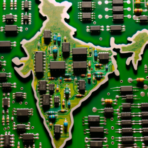
India isn't only planning to produce semicon chips, but also the equipment required for their production, according to IT Minister Ashwini Vaishnaw. The goal of India is to produce every resource required for the production of semiconductors, including fabs, chemicals, and equipment. According to IT Minister Ashwini Vaishnaw, producing equipment for making chips will significantly enhance India's reputation in the global semiconductor industry.
India is preparing to create its own equipment for manufacturing semiconductors, as reported by IT Minister Ashwini Vaishnaw. While inaugurating the Applied Materials' India Validation Centre in Bengaluru, Vaishnaw stressed that India will begin to produce all the necessary components for semiconductor production, such as fabs, chemicals, and machinery.
Applied Materials has put $20 million into the center, which is set to hire 500 employees, according to an Economic Times report.
The IT minister asserted that the complete semiconductor infrastructure, including fabrication units, assembly, testing, marking, and packaging units, chemicals, gases, substrates, consumables, and equipment used in semiconductor production, will be manufactured in India.
Furthermore, Applied Materials disclosed plans to invest $400 million over a period of four years to set up a semiconductor manufacturing technology engineering hub in Bengaluru.
The minister also noted that the deals struck during the Prime Minister's trip to the US have been fulfilled. This includes the beginning of the ATMP construction by Micron and the launch of Semiverse Solutions by LAM Research for training in semiconductor engineering.
In addition, Applied Materials plans to set up a facility in India as per the agreements, and AMD has opened a design centre in Bengaluru. These advancements signify substantial growth in India's semiconductor sector.
Sonny Kunnakkat, who is the managing director of Advanced Manufacturing Technology at Applied Materials' Global Operations, announced that the recently set up unit in India would be the first privately owned facility capable of handling 300 mm wafers. This is a notable progression from the earlier 200 mm wafer processing capabilities in the nation.
The Indian Institute of Technology (IIT Kunnakkat) has recognized that it has a 300 mm processing plant, but it's important to note that this new plant is for business use, not educational purposes. Applied Materials will carry out its own research and development at this facility, concentrating on tools for chip production. The wafers that are produced will not be sold, instead, they will be used internally to assist their clients in manufacturing chips.
Kunnakkat emphasized the fast-paced advancements in equipment, which require constant innovation to meet the changing demands of customers. He insisted that this ongoing progression will be a primary concern at the new establishment.
Kunnakkat pointed out that the semiconductor hardware system in India is still in its early stages. He stressed the importance of a well-rounded support system, which includes aspects like supply chain management, material handling, logistics, and basic utilities such as water and electricity, to guarantee the endurance and lifespan of semiconductor factories within the nation.
He also highlighted the need for cooperation between ecosystem participants to expand semiconductor production in India, underlining the essential need for larger-scale facilities to satisfy industry requirements. Applied Materials is actively collaborating with the government to aid in this expansion process.
Kunnakkat elaborated on the process of setting up the company's engineering centre in Bengaluru, stating, "We have a ten-acre plot where we plan to construct it. The facility is complex and is still in the design phase. Currently, we lack staff in India to design such a facility. We are therefore gathering expertise from various global locations. However, this won't be completed in the upcoming six months."
Kunnakkat emphasized the lack of a system development approach and insufficient experience in setting up and starting semiconductor tools in India. He noted that the firm had to employ specialists from Singapore and Taiwan, who are experts in these operations, to work at its India Validation Centre.
(Incorporating information from various sources)
Look for us on YouTube
Top Programs
Relevant Articles
2024 Rising Bharat Summit: An Indian manufactured semicon is slated for a marketplace debut in Dec 2024, according to IT Minister Ashwini Vaishnaw
2024 Rising Bharat Summit: India has emerged as a significant export center, however, Congress squandered 40 years, as stated by IT Minister Ashwini Vaishnaw
Indian Government gives green light to Tata Group's Rs 91,000 crore chip factory to be established in Gujarat's Dholera
IT Minister, Rajeev Chandrasekhar states the next innovation wave in India will stem from semiconductors and AI
2024 Rising Bharat Summit: IT Minister Ashwini Vaishnaw confirms that an Indian produced semicon will be launched in the market by Dec 2024
2024 Rising Bharat Summit: IT Minister Ashwini Vaishnaw states India has become an important export hub and criticizes Congress for losing four decades
Indian Government sanctions Tata Group's proposal for a Rs 91,000 crore chip foundry to be located in Dholera, Gujarat
Rajeev Chandrasekhar, IT Minister, anticipates the next surge of innovation in India to originate from semiconductors and AI
Can be found on YouTube
All rights reserved by Firstpost, Copyright 2024.


+ There are no comments
Add yours