


Activities
Divisions
Performances
Activities
Divisions
Performances
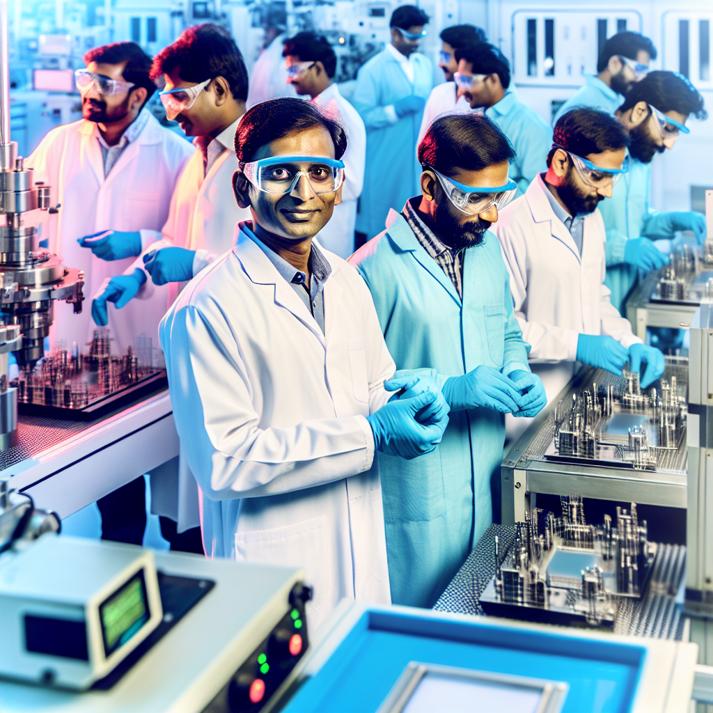
India is set to begin production of not only semiconductor chips but also chip-making machinery, according to IT Minister Ashwini Vaishnaw. The nation's goal is to produce all the required elements for semiconductor fabrication, encompassing fabs, chemicals and equipment. Vaishnaw expressed that the manufacture of chip-making machinery will significantly enhance India's standing in the global semiconductor industry.
IT Minister Ashwini Vaishnaw has announced that India is preparing to produce its own semiconductor manufacturing tools. During the inauguration of the Applied Materials' India Validation Centre in Bengaluru, Vaishnaw emphasized that India will be responsible for creating all components required for the production of semiconductors, such as fabs, chemicals, and equipment.
Applied Materials has put $20 million into the center, which is expected to provide jobs for 500 individuals, according to a report from the Economic Times.
The IT minister asserted that the whole semiconductor infrastructure, including fabs, ATMP units, chemicals, gases, substrate, consumables, and equipment for semiconductor production, will all be manufactured in India.
Furthermore, Applied Materials has disclosed plans to invest $400 million over a span of four years to set up a semiconductor manufacturing technology engineering hub in Bengaluru.
The minister also highlighted that the deals struck during the Prime Minister's trip to the US have been successful. These include the start of Micron's ATMP construction and the launch of LAM Research's Semiverse Solutions for training semiconductor engineers.
Additionally, Applied Materials plans to set up a facility in India according to the agreements, and AMD has launched a design center in Bengaluru. These advancements indicate substantial growth in India's semiconductor sector.
Sonny Kunnakkat, who is the managing director of Applied Materials’ Advanced Manufacturing Technology, Worldwide Operations, announced that the newly built facility in India will be the first privately-owned one capable of handling 300 mm wafers. This marks a substantial upgrade from the country's earlier capability of processing 200 mm wafers.
Recognizing that a 300 mm processing unit is operational at the Indian Institute of Technology (IIT), Kunnakkat stressed that this new unit is for business purposes instead of educational ones. Applied Materials will carry out its own research and development in this facility, concentrating on tools for chip production. The wafers generated will not be marketed, but will be utilized internally within the company's machinery to assist its clients in chip fabrication.
Kunnakkat emphasized the fast pace at which equipment is changing, which demands constant progress to meet the changing needs of the customer. He insisted that such progress will be a major emphasis at the new establishment.
Kunnakkat pointed out that India's system for semiconductor hardware is still in its early stages. He stressed the importance of a full-fledged support system, which includes managing the supply chain, handling materials, logistics, and crucial utilities such as water and electricity, to guarantee the durability and long-term survival of semiconductor factories in the nation.
He additionally stressed the significance of cooperation among ecosystem participants to expand semiconductor production activities in India, highlighting the need for such establishments on a grand scale to satisfy industry requirements. Applied Materials is actively collaborating with the government to aid this expansion procedure.
Kunnakkat elaborated on the activation process of the firm's engineering hub in Bengaluru, stating, "Our plans are to construct it on a ten-acre plot we own. The centre's design is complex and is currently in progress. At the moment, we lack the necessary design expertise in India. We're importing knowledge from various global regions. However, this won't be accomplished within the next half year."
Kunnakkat emphasized that India lacks a systematic approach to engineering and little experience in setting up and initiating semiconductor tools. He noted that the company had to recruit experts from Singapore and Taiwan, who are proficient in these duties, to operate in its India Validation Centre.
(Incorporating information from various sources)
Look for us on YouTube
Highlighted Programs
Associated Articles
In the Rising Bharat Summit 2024, IT Minister Ashwini Vaishnaw announced that Indian-manufactured Semicon will be available in the market by December 2024.
In the same summit, Vaishnaw stated that India has become a significant export center, but accuses the Cong of wasting four decades.
The Indian government has given the green light to Tata Group's Rs 91,000 crore chip foundry, which will be established in Dholera, Gujarat.
IT Minister Rajeev Chandrasekhar predicts that the forthcoming wave of innovation in India will predominantly come from semicon and AI.
These news can be found on YouTube.
Firstpost holds the exclusive rights, reserved until 2024.


+ There are no comments
Add yours