


Happenings
Divisions
Programs
Happenings
Divisions
Programs
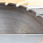
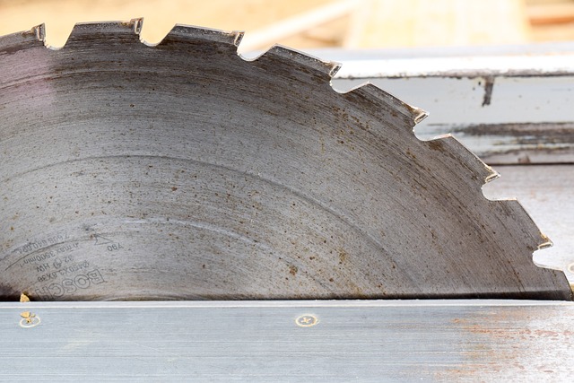
TSMC considering the possibility of establishing a state-of-the-art chip manufacturing facility in Japan
Taiwan's TSMC is aiming to broaden its horizons beyond Taiwan and is considering the establishment of a high-level silicon packaging facility in Japan. The semiconductor titan is planning to implement chip-on-wafer-on substrate (CoWoS) packaging technology in the nation.
According to insider information, Taiwan Semiconductor Manufacturing Co, also known as TSMC, is said to be considering the establishment of a sophisticated silicon packaging facility in Japan. This move could potentially indicate a significant step forward in the attempts to rejuvenate Japan's semiconductor sector.
The talks are still in their early phases, according to insiders who prefer to stay unnamed due to the confidential status of the data. The semiconductor giant is considering introducing its chip-on-wafer-on-substrate (CoWoS) packaging technology to Japan, as one informed individual disclosed.
CoWoS, an innovative technology, involves layering chips on top of each other. This not only increases processing power but also saves space and lowers power usage. Currently, all of TSMC's CoWoS capacity is located in Taiwan. The source stated that no concrete decisions about the extent or schedule of possible investments have been made yet. TSMC, earlier recognized as Taiwan Semiconductor Manufacturing Co., refrained from making any comments on this issue.
The rise in artificial intelligence has led to an increased worldwide need for sophisticated semiconductor packaging. This has caused chip manufacturers such as TSMC, Samsung Electronics, and Intel to boost their production capabilities.
In January, the CEO of TSMC, C.C. Wei, unveiled a strategy to increase CoWoS production twofold within the year, with additional growth expected by 2025. In addition, TSMC revealed plans to boost the output of advanced packaging in Chiayi, in the south of Taiwan, in response to strong market demand. However, they did not provide specifics.
The building of a new CoWoS facility in Chiayi is set to begin in early May, according to quotes from Vice Premier Cheng Wen-tsan, as reported by Taiwan's Central News Agency.
TSMC is looking to expand its presence in Japan by enhancing its advanced packaging capabilities. The company recently opened one facility and announced plans for another, both located on the southern island of Kyushu, a crucial center for chip production. TSMC has established collaborations with companies like Sony and Toyota, and the total investments in the Japanese project are expected to surpass $20 billion.
In addition, TSMC set up a state-of-the-art packaging research and development hub in the Ibaraki region, to the northeast of Tokyo, in 2021. With Japan's strong foundation in semiconductor materials and equipment, along with increasing investments in chip manufacturing capabilities and a dependable clientele, the nation is well-positioned to take on a more significant role in advanced packaging, as mentioned by a high-ranking authority at Japan's industrial ministry.
Analyst Joanne Chiao from TrendForce has warned that TSMC's possible venture into advanced packaging in Japan may be limited in its scope, given the unclear demand for CoWoS packaging in Japan. Chiao further noted that most of TSMC’s present CoWoS customers are located in the United States.
So far, TSMC's efforts in Japan have been backed by significant financial support from the Japanese government. This is because the government sees semiconductor production as a crucial part of its economic stability, particularly after experiencing challenges with South Korea and Taiwan.
At the same time, it's been reported that Intel is considering setting up a state-of-the-art packaging research center in Japan. This move is aimed at enhancing its cooperation with local semiconductor supply companies, as per insiders. On the other hand, Samsung is in the process of establishing a similar facility in Yokohama, which is situated to the southwest of Tokyo, and this project has the support of the government. Furthermore, the South Korean chip manufacturer is in talks with Japanese and other firms about sourcing materials as it seeks to utilize packaging technology to improve its standing in the high-bandwidth memory chip market, as stated by Reuters.
(Incorporating information from various sources)
Look for us on YouTube
Prime Programs
Associated Narratives
can be found on YouTube
Firstpost holds all rights reserved, protected by copyright in 2024.


+ There are no comments
Add yours