


Occurrences
Divisions
Productions
Occurrences
Divisions
Productions
TSMC considering possibilities to establish an advanced chip-making facility in Japan
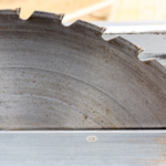
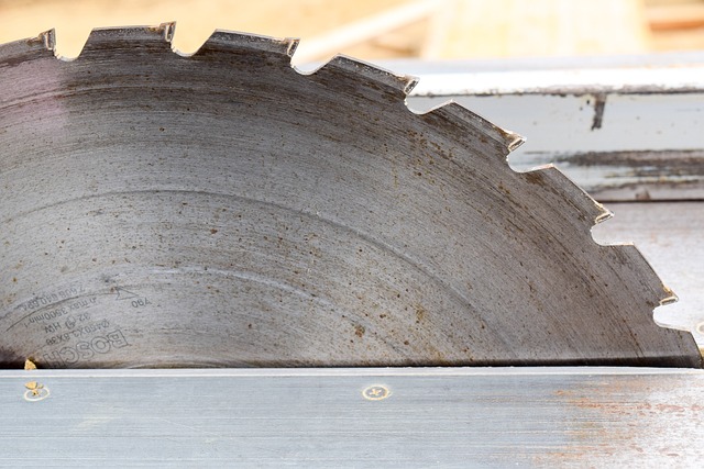
TSMC from Taiwan is contemplating spreading its operations beyond Taiwan and aims to establish a high-tech silicon packaging facility in Japan. The semiconductor giant plans to install a chip-on-wafer-on substrate (CoWoS) packaging technology in the nation.
TSMC, also known as Taiwan Semiconductor Manufacturing Co, is supposedly contemplating establishing a sophisticated silicon packaging facility in Japan, according to insiders. This move could signify a considerable step towards the regeneration of Japan's semiconductor sector.
Conversations are currently in their initial phases, according to informants who chose to stay unnamed due to the confidential status of the details. The semiconductor giant is considering introducing its chip-on-wafer-on-substrate (CoWoS) packaging technology to Japan, as disclosed by an individual with knowledge of the situation.
CoWoS, an advanced technology, involves layering chips on top of each other, thus improving processing power and saving space as well as energy. At this time, TSMC's entire CoWoS capacity is located in Taiwan. The source stated that no final decisions about the size or timing of possible investments have been made. TSMC, previously referred to as Taiwan Semiconductor Manufacturing Co., declined to comment on the issue.
The increased need for sophisticated semiconductor packaging worldwide has risen alongside the growth in artificial intelligence, leading chip manufacturers such as TSMC, Samsung Electronics, and Intel to boost their production capabilities.
In January, CEO of TSMC, C.C. Wei, declared intentions to increase CoWoS production by 100% within the year, and has further growth planned for 2025. Additionally, TSMC revealed plans to enhance advanced packaging capacity in Chiayi, located in southern Taiwan, in response to strong market demand, although no specific details were provided.
The building of a new CoWoS facility in Chiayi is set to begin in early May, according to statements made by Vice Premier Cheng Wen-tsan and reported by Taiwan's Central News Agency.
TSMC is looking to expand its presence in Japan by enhancing its high-tech packaging abilities. The company recently opened one facility and declared the establishment of another, both located on Kyushu island, a critical center for chip production. TSMC has also formed alliances with companies like Sony and Toyota, with the overall investments in the Japanese project expected to surpass $20 billion.
In addition, TSMC set up a high-tech packaging research and development hub in the Ibaraki region, to the northeast of Tokyo, in 2021. The strong semiconductor materials and equipment infrastructure in Japan, along with increasing investments in chip manufacturing capacity and a reliable customer base, put the country in a good position to take on a bigger role in advanced packaging, as remarked by a high-ranking official from Japan's industry ministry.
TrendForce analyst Joanne Chiao warned that TSMC's possible high-tech packaging venture in Japan could be limited in size due to the unclear demand for CoWoS packaging in the country. She further mentioned that the majority of TSMC's existing CoWoS clients are located in the United States.
So far, TSMC's efforts in Japan have been significantly supported by the Japanese government's heavy subsidies. This is because Japan considers semiconductor production as a crucial part of its economic security, especially after experiencing challenges in competing with South Korea and Taiwan.
At the same time, it has been reported that Intel is considering setting up a sophisticated packaging research center in Japan to enhance partnerships with local semiconductor supply chain companies, based on information from those in the know. On the other hand, Samsung is in the process of establishing a similar research center in Yokohama, which is southwest of Tokyo, with support from the government. The South Korean semiconductor manufacturer is also in talks with Japanese and other businesses about acquiring materials as it tries to take advantage of packaging technology to keep pace in the high-bandwidth memory chips industry, according to a report by Reuters.
(Incorporating information from various sources)
Search for us on YouTube
Prime Programs
Connected Narratives
can be found on YouTube
All rights preserved by Firstpost, Copyright 2024.


+ There are no comments
Add yours